|
IN BRIEF
|
In the electrifying world of technology, printed circuit boards (PCBs) serve as the backbone of countless devices, transforming intricate designs into innovative functionality. Designing and manufacturing a PCB is an art form, requiring a blend of intricate engineering and cutting-edge technology. It all begins with a spark of inspiration, where ideas are translated into sophisticated schematics. Skilled engineers utilize advanced CAD/CAM software to craft the perfect layout, paving the way for the magic that follows. Just imagine layers of conductive materials intricately etched onto an insulating substrate, forming pathways that enable seamless communication between electrical components. The journey from concept to creation is a fascinating dance of precision and creativity that ultimately brings our devices to life.

How Printed Circuit Boards Are Designed
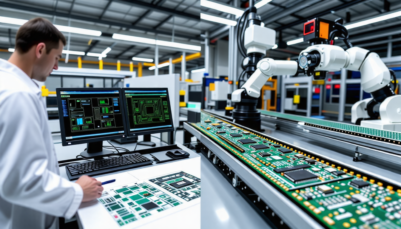
The design of printed circuit boards (PCBs) is a critical step that ensures all electronic components work harmoniously. The process begins with creating a comprehensive schematic diagram. This visual representation outlines the electronic connections and component placement, guiding further steps in the design process. Engineers typically use CAD (Computer-Aided Design) software to draft and simulate the intended circuit layout.
Schematic Diagram Creation
During the schematic creation, designers meticulously plan where each component will be placed on the PCB, ensuring that signal paths are optimized for performance. This involves selecting the appropriate electrical components, such as resistors, capacitors, and integrated circuits, while considering their specifications and compatibility.
Component Layout and Design Rules
Once the schematic is complete, the next step involves laying out the PCB. This stage requires adhering to design rules, which ensure the functionality and manufacturability of the circuit board. Factors such as trace width, spacing, and component orientation are crucial. Proper layouts prevent interference between components and minimize signal loss, thus enhancing performance.
Design Verification
After the layout is finalized, it undergoes rigorous verification. Design Rule Check (DRC) tools within the CAD software help identify potential issues, such as overlapping traces or invalid component placements. This step is vital for catching discrepancies early, preventing costly modifications during manufacturing.
From Design to Production
Moving from design to actual production requires translating the completed PCB layout into files that can be interpreted by manufacturing equipment. The Gerber files generated from the CAD software include all necessary information about layers, drill holes, and component placements.
File Preparation and Processing
The next step involves processing these files into a format usable for production. This often includes generating additional files for layers, solder masks, and silkscreen prints that provide instructions for how to assemble the components during manufacturing.
Panelization
Manufacturers do not produce a single PCB; instead, they create multiple boards on a larger sheet known as a panel. This process, called panelization, maximizes efficiency and minimizes waste. The panels are designed to contain several identical PCBs, which will be separated later in the manufacturing process.
The PCB Manufacturing Process
The manufacturing of printed circuit boards encompasses several well-defined steps, each contributing to the creation of a high-quality final product. Understanding these processes helps to appreciate the intricate nature of PCB production.
Material Selection
The foundation of any PCB is the substrate material, which serves as an insulator and provides structure. Common choices include FR-4, a fiberglass material, and polyimide for flexible boards. The choice of material impacts the board’s thermal properties and overall durability, influencing its performance in various applications.
Layer Fabrication
Once materials are chosen, the fabrication of the individual layers begins. Manufacturers create inner layers by applying a thin layer of copper to the substrate. The excess copper is then etched away in a process that leaves behind distinct traces, which will later connect the electronic components.
Photoresist Application
To etch the copper accurately, a photoresist material is applied to the copper layers. This material hardens when exposed to UV light, allowing manufacturers to define the areas that should remain copper and those that should be removed. After exposure, the unexposed areas are washed away, allowing for precise etching.
Drilling and Through-Hole Plating
Once the copper layers are set, the next step involves drilling holes for through-hole components and vias that connect different layers. Following drilling, a process called through-hole plating is employed to deposit a conductive material inside the holes, ensuring reliable electrical connections between layers.
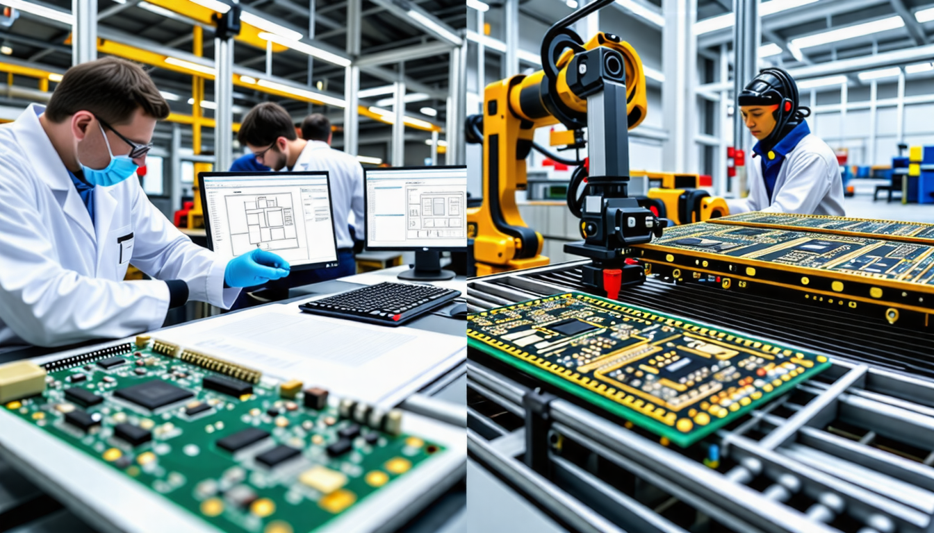
Assembly and Soldering Processes
With the layers fabricated and drilled, the assembly process begins. This phase requires precision and careful handling to ensure that all components are mounted accurately on the PCB.
Solder Paste Application
Before components are placed, solder paste is applied to the board. This paste is critical as it provides the necessary conductivity once heated. It is applied using a that corresponds to the pad locations for each component, ensuring no paste is wasted.
Component Placement
After solder paste application, components are strategically placed on the board. Automated machinery often aids in this process, utilizing pick-and-place technology to position components accurately within seconds. However, for more complex or larger components, manual placement may be necessary.
Reflow Soldering
Once components are placed, the PCBs proceed to the reflow soldering phase, where the entire board is heated to melt the solder paste, creating permanent connections. This step is accomplished in a specialized oven that carefully controls the heating profile to avoid damaging components while ensuring that all solder connections are made.
Testing and Quality Control
With the assembly complete, rigorous testing kicks in to ensure the quality and functionality of the PCBs. Various methods are utilized to check for defects and ensure each board meets stringent quality standards.
Electrical Testing
Electrical tests are performed to verify the integrity of connections and components. This may include in-circuit testing, which measures each connection in the circuit independently, confirming the layout functions as intended.
Visual Inspection
In addition to electrical tests, visual inspections are crucial. Technicians visually examine boards for any soldering defects, component misalignment, or damages. Automated Optical Inspection (AOI) systems may also be employed to enhance efficiency and accuracy in this step.
Final Packaging and Shipping
Once testing is complete, the final stage involves packaging the PCB for shipment. Proper packaging is essential to prevent damage during transit, ensuring that the circuit boards arrive at their destination in perfect condition, ready for integration into electronic devices.
The design and manufacturing of printed circuit boards is a complex and multi-faceted process. Each step, from initial layout to final testing, plays an integral role in producing high-quality boards that serve as the backbone of modern electronics. Understanding these stages not only highlights the engineering marvel of PCB production but also emphasizes the precision and care required throughout the entire process.
Understanding how printed circuit boards (PCBs) are designed and manufactured is essential for innovation in electronics. The journey begins with a detailed schematic diagram, where engineers utilize advanced CAD/CAM software to define the circuit layout and component placement. According to recent industry reports, the demand for PCBs is projected to grow by 4.5% annually, emphasizing the need for efficient design practices.
Following the design phase, the transition to fabrication occurs. During this step, a thin layer of conductive material is applied to an insulating substrate, forming the actual circuit. The process involves intricate techniques such as laser printing to create negative photo films, ensuring precise etching of copper layers. This delicate operation leaves behind the intended copper traces crucial for electrical connectivity.
Interestingly, PCBs are manufactured in large arrays, known as panels, which allows for economies of scale. Each plate undergoes several steps, culminating in attaching components through soldering, providing both electrical connectivity and mechanical stability. With the increasing complexity of electronic devices, mastering the PCB manufacturing process is vital, as it directly influences reliability and performance.

The journey of printed circuit boards (PCBs) begins with intricate designs capturing the schematics of electronic connections. Using advanced CAD/CAM software, engineers layout component placements, ensuring precision and efficiency. The initial designs are converted into physical forms through a series of meticulous processes, including the creation of negative photo films with laser printing, followed by the etching of copper layers on a substrate material. As the manufacturing progresses, copper traces emerge, linking electrical components securely to conductive pads. Each step, from design verification to the final artwork, plays a crucial role in producing functional circuits that power our modern world. The artistry behind PCBs reflects innovation and technical prowess, bridging the gap between vision and reality.
FAQ
What is the first step in designing a printed circuit board?
R: The initial step involves creating a schematic diagram, which outlines the electrical components and their connections. This design serves as the blueprint for the circuit board.
How are the layers of a PCB created?
R: During the manufacturing process, several layers of copper are carefully etched to form the desired circuit traces. These layers include both inner and outer layers that will facilitate connections between components.
What software is typically used in PCB design?
R: Most designers utilize CAD/CAM software for PCB design. This software helps in laying out the components and routing the electrical connections effectively.
How does the manufacturing process start?
R: The manufacturing process begins by converting the design files into film negatives, which are then used to print the inner layers of the PCB.
What materials are used to create a printed circuit board?
R: A typical PCB is made from a combination of substrate material for insulation and a thin layer of conductive material, usually copper, which facilitates the electrical connections.
