|
IN BRIEF
|
Embarking on the journey of PCB assembly can feel daunting, yet the satisfaction derived from creating your own electronic devices is unparalleled. This step-by-step guide will illuminate the intricate and fascinating world of circuit board assembly. From the initial planning stages where conceptualization begins, to the precise placement of components, every phase is an exhilarating mix of art and science. Understanding the essential techniques, standards, and tools involved in the PCB assembly process will empower you to navigate through the complexities with confidence. Whether you’re a novice or a seasoned pro, this guide is your key to mastering the intricate dance of components on a printed circuit board.
Understanding the PCB Assembly Process
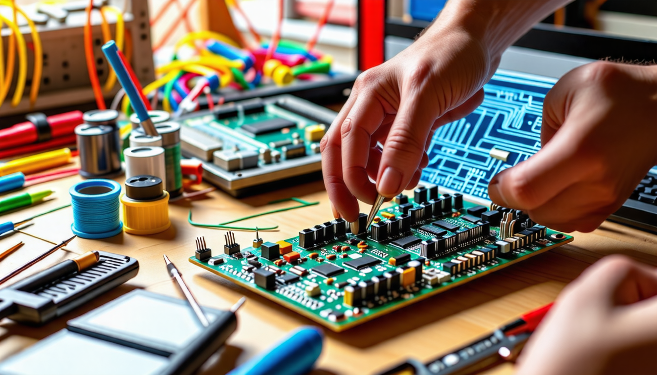
Assembling a printed circuit board (PCB) for electronic devices involves a series of methodical steps that culminate in a functional and efficient circuit. This detailed process encompasses various techniques and standards, each crucial for ensuring reliability and performance. Gaining insights into the PCB assembly process equips you with the necessary skills and knowledge to create effective electronics.
Preparing for Assembly
The first stage in PCB assembly requires adequate preparation. This includes gathering essential files such as the Gerber files, Bill of Materials (BOM), and production documents. Each of these elements provides vital information regarding component specifications and layout requirements for the PCB. Ensuring everything is in order facilitates a smoother assembly process and mitigates potential errors.
Conduct a DFA Check
Before proceeding, it is advisable to conduct a Design for Assembly (DFA) check. This step scrutinizes the design elements to ascertain their suitability for efficient assembly and identifies any potential challenges that might arise. A thorough DFA assessment can prevent costly modifications later in the process and ensure components are compatible with assembly techniques.
Component Selection
Choosing the appropriate components for your PCB is pivotal. It influences not only the board’s performance but also its overall cost and efficiency. Different components serve various purposes ranging from resistors and capacitors to integrated circuits and connectors. Evaluate these components based on suitability, availability, and cost before finalizing the BOM.
Understanding Component Types
During the selection phase, it’s crucial to understand the various types of components involved in the assembly. Some components are surface mount technology (SMT), while others are through-hole. SMT components are placed directly onto the surface of the PCB, whereas through-hole components involve inserting leads into holes and securing them from the opposite side. Recognizing these types will inform your assembly approach.
Creating the PCB Layout
The layout is another critical aspect of PCB assembly. A well-structured layout ensures that the components will fit together correctly and interact as intended. Layout software is typically used to design the schematic and arrange the components. The goal is to create a functional and visually appealing board that adheres to engineering standards.
Using PCB Design Software
Numerous PCB design software options exist, each offering various tools for creating layouts. Popular choices include Altium Designer, Eagle, and KiCAD. These programs facilitate the drawing of schematics, establishing electrical connections, and finalizing the PCB design. Familiarity with the chosen software is essential for efficiency throughout the design phase.
Soldering Techniques in PCB Assembly
Soldering is an indispensable part of the PCB assembly process. This technique involves melting solder to create a bond between the components and the PCB. Different methods exist, each with its own applications suited to specific assembly needs.
Manual Soldering
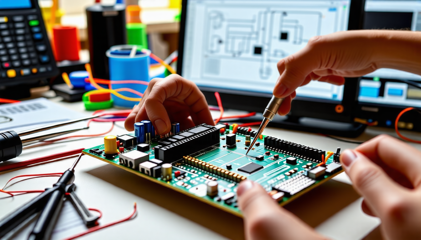
For projects that involve smaller quantities of PCBs, manual soldering is often preferred. This technique allows for greater control over the soldering process, making it ideal for delicate components. It requires a soldering iron and solder to attach the components securely to the board. While time-consuming, manual soldering enables precise placement and careful handling of sensitive parts.
Automated Soldering**/h3>
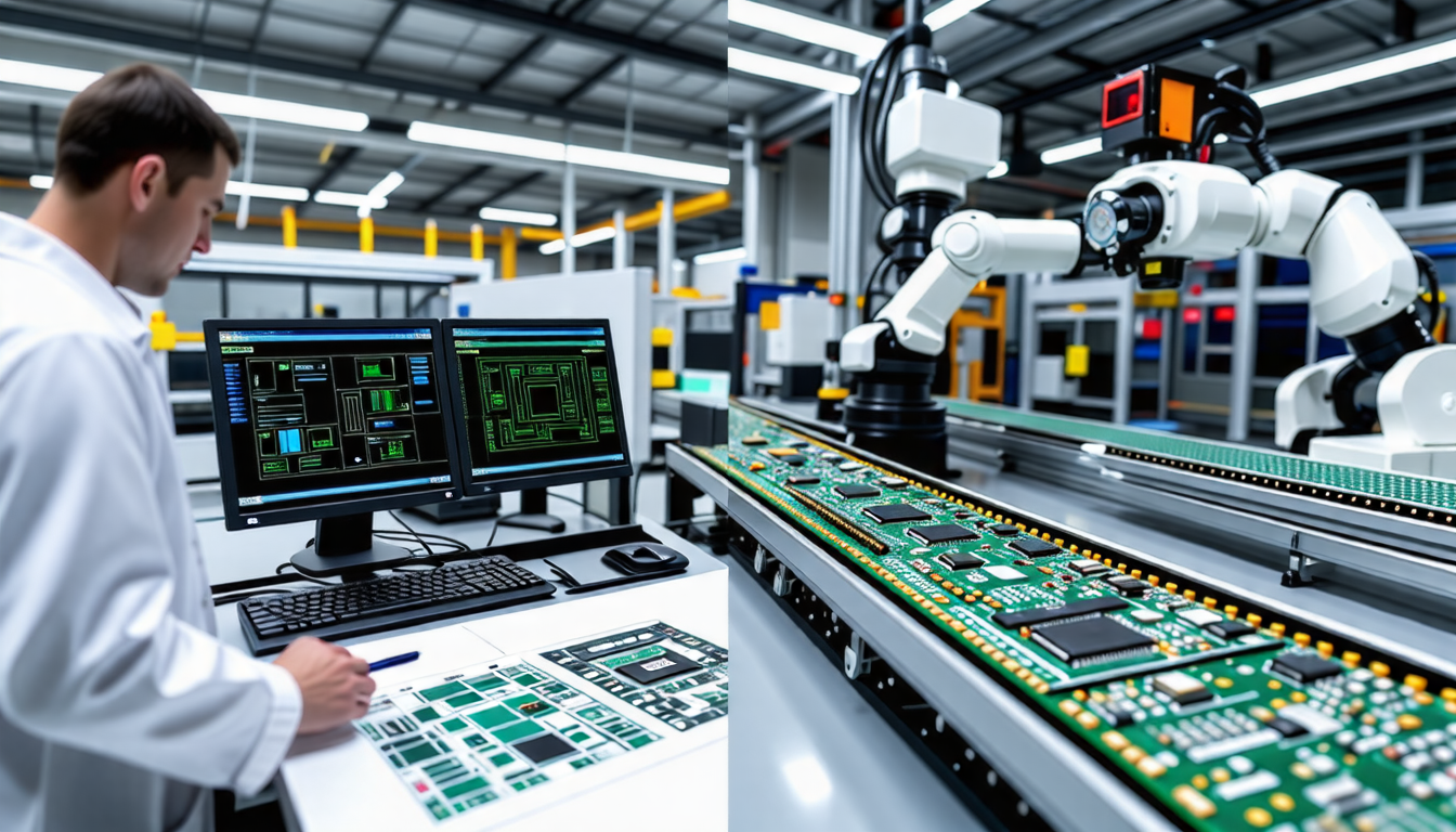
In contrast, automated soldering techniques, including wave soldering and reflow soldering, are typically used in mass production. Wave soldering involves passing the PCB over a wave of molten solder, while reflow soldering entails heating the solder paste applied to the components, causing it to melt and create connections when cooled. These automated processes increase efficiency and ensure uniform connections across multiple boards.
Placement of Components
Once the components are selected and soldering techniques are understood, the next step is the placement of components onto the PCB. Proper arrangement is critical to avoid overcrowding and ensure easy access for soldering and testing.
Surface Mount Component Placement
For surface mount components, placement should be precise to avoid misalignment during soldering. Using automated pick-and-place machines can significantly enhance accuracy and speed while reducing the risk of human error. Make sure to follow the component polarity guidelines and keep the orientation consistent.
Through-Hole Component Placement
For through-hole components, ensure they are inserted into the designated holes correctly. It’s important to double-check that the component leads align properly with the holes to avoid bending, which can complicate soldering. Once placed, the components are typically secured with a light hand pressure to hold them in place before soldering.
Conducting Testing after Assembly
Testing the PCB after assembly verifies the functionality of the electronic device. This quality assurance step is essential, as it can uncover issues that might not become apparent during the assembly process.
Initial Visual Inspection
Start with a thorough visual inspection of the assembled PCB. Look for solder bridges, misaligned components, or any visible damage. This initial check helps identify glaring issues before proceeding to the more rigorous testing methods.
Functional Testing
After the visual inspection, conduct functional testing to ensure the PCB operates as intended. This can include applying power to the circuit, measuring voltages at various points, and checking for correct response to inputs. Utilizing automated test equipment can streamline this process and provide precise measurements.
Final Inspection and Quality Control
A final inspection is necessary to conclude the assembly process. This ensures every aspect of the PCB aligns with project specifications and quality standards.
Documentation and Compliance
After assembly and testing, document the assembly process and any findings from the inspections and tests. This documentation not only serves as a record for future reference but also assists in demonstrating compliance with industry standards. Quality control plays a significant role, requiring that all boards meet established criteria.
Packaging and Distribution
Finally, once the PCBs pass inspection, they are carefully packaged for distribution. Proper packaging is essential to protect the boards from damage during transit, which could compromise function. Employ anti-static materials and cushioning to safeguard against physical shocks and electrical discharge.
Resources and Further Learning
For those wishing to deepen their understanding of PCB assembly, numerous resources are available online. Comprehensive guides break down PCB design and manufacturing processes thoroughly. Companies that specialize in electronic design and production may offer valuable insights, techniques, and best practices that enhance your skills. A great resource to explore includes this detailed article on how printed circuit boards are designed and manufactured.
Embracing Innovation and Best Practices
The electronics field is ever-evolving, with continual advancements and trends. Keeping up-to-date with current technologies, tools, and techniques allows you to optimize your PCB assembly process, ensuring high-quality results that meet modern demands. Embracing innovative practices not only refines the assembly process but can also open new avenues for creativity in electronic design.
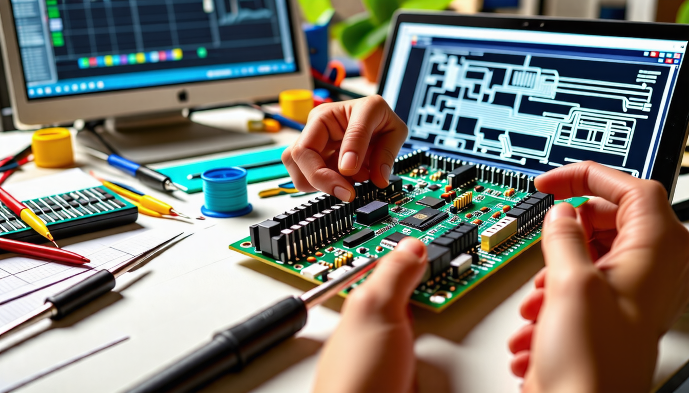
Assembling a PCB for electronic devices is an intricate yet rewarding process. It all begins with proper design; a well-structured schematic ensures that components are aligned and connected efficiently. Reports indicate that nearly 80% of issues in PCB performance stem from design flaws, underscoring the importance of meticulous planning.
The next crucial step involves selecting the right components. A typical PCB assembly might include over 30 different parts, ranging from resistors to microcontrollers. Consequently, ensuring a comprehensive BOM (Bill of Materials) is essential in minimizing production delays and reducing costs by up to 20%.
After components are selected, the actual assembly process kicks off. Techniques such as Surface Mount Technology (SMT) and through-hole soldering come into play. SMT generally allows for a more compact design and can reduce manufacturing time by approximately 25%, thus making it a popular choice among engineering teams.
Once assembled, testing is paramount. It is estimated that about 10% of PCBs fail in the initial testing phase, which emphasizes the necessity of rigorous quality control measures. By adhering to these steps, teams not only enhance product reliability but also ensure optimal performance of electronic devices.
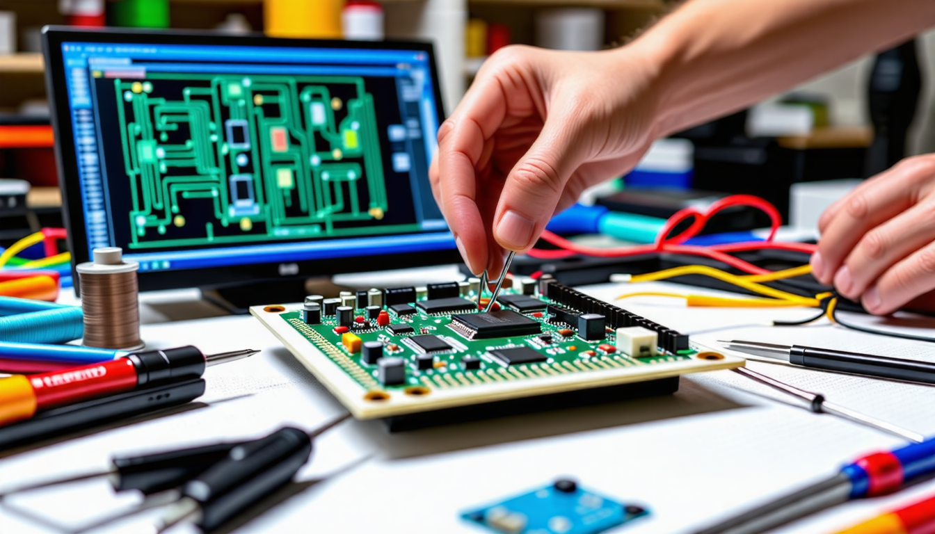
Assembling a PCB for electronic devices may seem daunting, but breaking it down into manageable steps can simplify the process. Start by preparing essential files such as the Gerber data and Bill of Materials (BOM). This preparation is crucial for ensuring a seamless assembly workflow. Next, focus on the placement of components, carefully sorting them into either through-hole or SMT categories based on your design. Following this, soldering the components securely to the board is vital, employing appropriate techniques to achieve strong connections. Don’t forget that testing and inspection are necessary stages to ensure functionality before the final product is complete. With practice and attention to detail, mastering PCB assembly becomes achievable!
FAQ
What is the first step in the PCB assembly process?
R: The first step in the PCB assembly process involves preparing the necessary files, such as the Gerber files, Bill of Materials (BOM), and production documentation to ensure a smooth assembly.
How do I select the components for my PCB?
R: To select components, consider the circuit design, the specifications required for each component, and compatibility with the other elements on the printed circuit board.
What soldering techniques should I use for PCB assembly?
R: Common soldering techniques for PCB assembly include manual soldering, wave soldering, and reflow soldering. The choice of technique depends on the complexity of the board and the components used.
How can I ensure the quality of my assembled PCB?
R: You can ensure quality by conducting inspections at various stages of the assembly, including visual checks, automated optical inspections, and functional testing to validate the performance of the circuit board.
What should I do if I encounter issues during PCB assembly?
R: If you encounter issues, first identify the root cause by reviewing the assembly process and checking for any discrepancies in the documentation or component placement. It may also be helpful to consult with experienced PCB manufacturers or references for troubleshooting.
