|
IN BRIEF
|
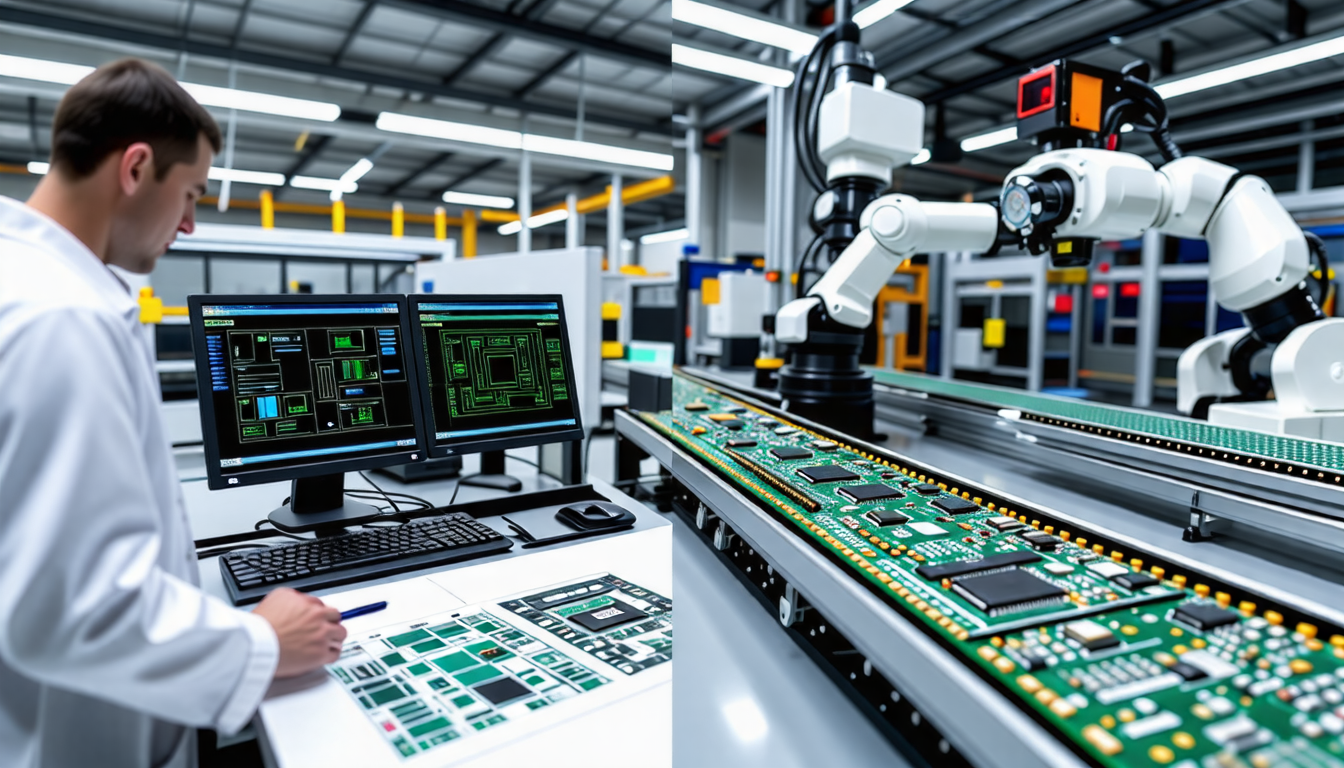
In the rapidly evolving world of electronics, printed circuit boards (PCBs) serve as the unsung heroes, orchestrating the harmony between a myriad of components. At the heart of every device lies a complex journey, where raw materials transform into sophisticated circuits. PCB fabrication is a meticulous process that combines artistry with engineering precision, allowing designs to leap from computer screens into tangible reality. This intricate endeavor unfolds through a series of well-defined stages, each crucial in ensuring functionality and reliability. From the initial spark of design to the final touches of assembly, understanding these processes unlocks a realm of possibilities for innovation and technology. Delve into the captivating world of PCB fabrication, where imagination meets engineering excellence, paving the way for future technological marvels.
Printed Circuit Boards (PCBs) are a fundamental component in modern electronics, serving as the backbone for various devices. The creation of these complex structures involves several intricate processes that transform a design concept into a functional board. Understanding these processes gives insight into the meticulous craftsmanship required to manufacture PCBs efficiently and effectively.
Conclusion—The Future of PCB Fabrication
As technology advances, the PCB fabrication process continues to evolve. Innovations such as advanced robotics in manufacturing and enhanced design software are paving the way for even greater precision and efficiency. Staying updated with emerging trends and techniques is essential for engineers and manufacturers involved in the PCB industry.
Understanding how the various stages of PCB fabrication interplay gives a comprehensive view of the complexities involved. The movement from design to final product isn’t just a linear progression but a detailed orchestration of science and creativity that results in the vital electronic components powering our devices today.
For more detailed inquiries and insights about PCB processes and sustainable practices in the industry, you can explore more information here.
Fabrication of the PCB
The actual manufacturing of the PCB begins with the creation of a rigid substrate material, typically made from fiberglass or a composite material, which forms the base of the board. Once the substrate is ready, the intricate image of the PCB design is transferred onto the surface. This crucial step involves several methods, including photo-engraving or direct laser writing, to form a precise replica of the design.
Etching
Once the image is positioned correctly, the next step in PCB fabrication is etching. This process removes unwanted copper from the surface of the board. The board is covered in a protective layer, typically a photoresist film, before being exposed to ultraviolet light which hardens specific areas. Unexposed areas are then washed away, allowing a specific copper layer to be exposed for the etching process. Afterward, the board is submerged in a chemical etchant that removes the excess copper, leaving behind the desired circuit design.
The process of PCB fabrication is pivotal in the electronics industry and consists of multiple stages that ensure the creation of high-quality circuit boards. Initially, the design phase involves translating conceptual ideas into actionable layouts using advanced PCB design software. It’s estimated that nearly 70% of the design iterations occur at this stage, reflecting the complexity and necessity of thorough planning.
Following the design, the next crucial step is the manufacturing phase, where various techniques such as etching and drilling are employed to transform raw materials into functional PCBs. In 2022, the global market for PCBs was valued at approximately $63 billion, showing a significant growth trajectory as demand for electronics skyrockets. It’s noteworthy that advancements in technologies like surface-mount technology (SMT) now dominate assembly processes, improving efficiency and minimizing size.
Finally, after the boards are manufactured, they undergo rigorous testing to identify any defects that could hinder performance. More than 90% of the manufactured boards are subjected to automated optical inspection methods, ensuring only the highest quality products reach consumers. This systematic approach in understanding PCB fabrication not only highlights the technological progress but also the essential role these processes play in delivering reliable electronic solutions. For more insights into PCB processes, visit this resource.
Understanding the processes involved in PCB fabrication is essential for anyone engaged in electronics, from designers to engineers. This intricate journey begins with detailed design stages, where creativity meets technical precision. The process advances through various manufacturing phases, including precise etching, drilling, and surface finishing, ultimately bringing the design to life. The assembly phase plays a crucial role, where components are carefully placed onto the boards, ensuring functionality. Rigorous testing guarantees that each circuit board meets quality standards before delivery. This multi-step process is not just about creating a product; it’s about building connections, enabling communication, and fostering innovation in technology. A deep comprehension of these stages empowers professionals to optimize designs for efficiency and performance.
FAQ
What is the first step in the PCB fabrication process?
R: The initial stage involves transferring the circuit design from the manufacturing files to the physical board. This ensures that the intricate circuitry is accurately represented.
How does the PCB design verification work?
R: PCB design verification is crucial to ensure that the design meets all specifications and requirements. This process often includes simulations and testing to avoid errors before moving on to fabrication.
What manufacturing processes are used in PCB fabrication?
R: Key processes in PCB fabrication include etching the copper layers, drilling holes for connections, and laminating the layers together. These processes collectively shape the physical structure of the board.
What is the role of testing in PCB manufacturing?
R: Testing is essential to ensure the integrity and functionality of the finished circuit boards. This can involve various techniques like electrical testing and visual inspection to catch any defects before they are delivered to customers.
How does the assembly process differ from fabrication?
R: While fabrication refers to creating the physical board, assembly involves populating the board with electronic components. This step may be performed manually or with the help of automated machines.
